1939Wireless assembling was started at its present Head Office's location as a private enterprise.
1948Established Metal Plating Division.
1949Started production of light electric parts and plating process.
1953Reorganized into a limited company (Taiyo Manufacturing Co., Ltd). Incorporated with capital stock of 500 thousand yen.
1958Completed semi-automated facilities at Joto Plant. Capital increased to 2.5 million yen.
1959Electro Polishing Plant completed. Installed a fully-automated facility at Joto Plant. Capital increased to 3.5 million yen.
1961Kadoma Plant completed.
1962Coating Plant completed.
Capital increased to 5.7 million yen.
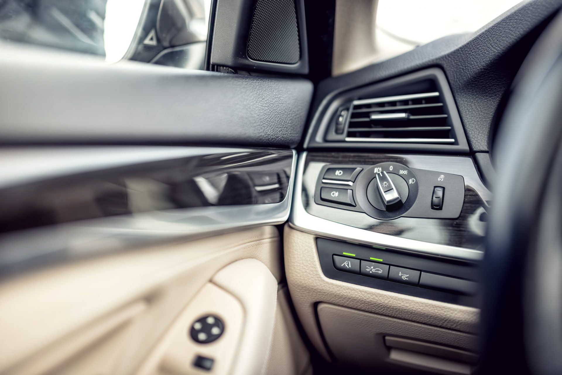
1964Non-Electrolytic Plating Plant established. Capital increased to 10 million yen. Mass production of plastics plating commenced.
1967Added another Non-Electrolytic Plating Plant. Capital increased to 16 million yen.
1968Press Plant completed. Capital increased to 21 million yen.
1969Capital increased to 30 million yen.
1971Capital increased to 46 million yen.
1972Established Knob Manufacturing Plant.
1973Capital increased to 49 million yen.
1974Closed Kadoma Plant and integrated to Joto Plant.
1976Non-Electrolytic Plating Plant was renamed to Synthetic Chemical Plant.
1977Press Plant, Knob Plant and Electro Plant integrated into Light Metals Plant.
Kozaburo Shikata assumed post of the President.
1979Capital increased to 83 million yen.
Zinc barrel plating line at Morishoji Plant integrated to Joto Plant.
1980Capital increased to 99 million yen.
1981Synthetic Chemical Product Plant refurbished and expanded.
1982Sakai Plant for molding line constructed.
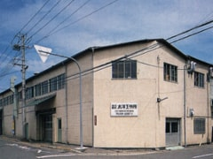
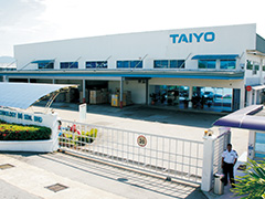
1983New Head Office building completed.
1984New Sakai Plant completed and a molding line was transferred to the new plant.
1986Kozaburo Shikata assumed post of the Chairman.
Takayuki Tsuji assumed post of the President.
1988Established R&D Center.
1989Completed first phase of the refurbish project of Metal Department.
1990Established Five "S" Department.
1991Established Taiyo Technology of America Inc.
1992Kozaburo Shikata decorated with the Fifth Order of the Sacred Treasure.
Completed the second-stage construction in Sakai Factory.
1993Completed new developmental product line at Sakai Division.
Established Taiyo Technology Singapore Pte Ltd at Jurong.
1994Started R&D Division at Sakai.
1995Completed second phase of rebuilding at Metal Department.
1994Started R&D Division at Sakai.
1998Established Taiyo Technology (MALAYSIA) Sdn Bhd.
1999TMC acquired ISO14001 certification.
2000Established Taiyo Soft Singapore Pte Ltd.
2001Metal Department changed its name to Tsurumi Division.
Established Taiyo Technology Portugal Componentes Plasticos Precisao.
Established automatic electro Au plating machine in Tsurumi Division.
2008Takayuki Tsuji assumed post of the Chairman.
Katsuyuki Tsuji assumed post of the President.
2009TMC acquired ISO27001 certification.
2010Shanghai Branch Office of Taiyo Soft Singapore Representative Office has opened in China.
2011Taiyo Technology System Thailand Inauguration.
Closed Taiyo Technology Portugal.
2012TAIYO- Technology -Industry: Thailand Inauguration.
2015Taiyo Technology System (Thailand) was incorporated
into Taiyo Technology Industry (Thailand).
2016Chemical and synthetic division acquired ISO/TS16949 certification.
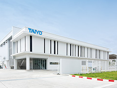
2017New Plating Plant completed at Taiyo Technology Industry (Thailand).
2018The chemical and synthetic division has acquired [ATF 16949 certification.